
 (585) 768-2513
Efforts to create reliable light-based quantum computing and quantum key distribution for cybersecurity could benefit from a Los Alamos National Laboratory study that demonstrates a new method for creating thin films to control single-photon emission.
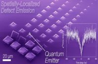
The approach exploits strain at highly spatially localized and spectrally well-separated defect emission sites, or tips, in the 750- to 800-nm regime in a tungsten/selenium film. The team synthesized the film through chemical vapor deposition using a multistep, diffusion-mediated gas source.
To separate the effects of mechanical strain from the substrate or dielectric-environment-induced changes in the electronic structure, the researchers created arrays of silicon dioxide tips with spatial dimensions on the order of 10 μm. The researchers used bending based on the small (about 4 nm) radius of the tips to impart electronic localization effects through morphology alone. The resulting strain was enough to change the electronic structure, but only at the tips. When the researchers transferred the film onto an array of silicon dioxide tips, they observed about an 87% yield of localized emission sites on the tips.
