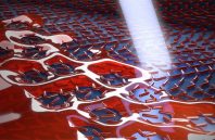
A way to produce glass metasurfaces that can be either rigid or flexible, developed by engineers from the EPFL Laboratory of Photonic Materials and Fiber Devices, could be used to fabricate all-dielectric optical metasurfaces quickly, at low temperatures, and with no need for a cleanroom. These metasurfaces could be used to build next-generation photonic circuits. Optical circuits, which are 10 to 100 times faster than electronic circuits and more energy-efficient, could transform the performance of many devices.
The new method employs dewetting, a natural process that occurs when a thin film of material is deposited on a substrate and then heated. The heat causes the film to retract and break apart into tiny nanoparticles.
The EPFL engineers used dewetting to create dielectric glass metasurfaces, rather than metallic metasurfaces. First, they created a substrate textured with the desired architecture. Then, they deposited the material — chalcogenide glass — in thin films just tens of nanometers (nm) thick. The substrate was heated for a couple of minutes until the glass became fluid and nanoparticles began to form in the sizes and positions dictated by the substrate’s texture.

 (585) 768-2513

